
I wanted to verify all my different assumptions and tool assisted calculations before I do further work on PCIe, SGMII* and Etehernet PCBs.
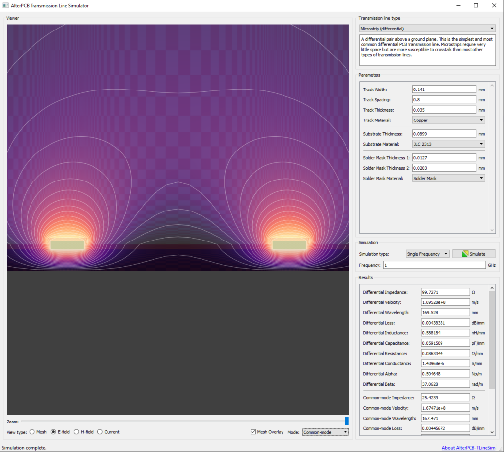
So I calculated the impedances with AlterPCB Transmission Line Simulator (also a nice view of the electric field regarding EMI etc…)
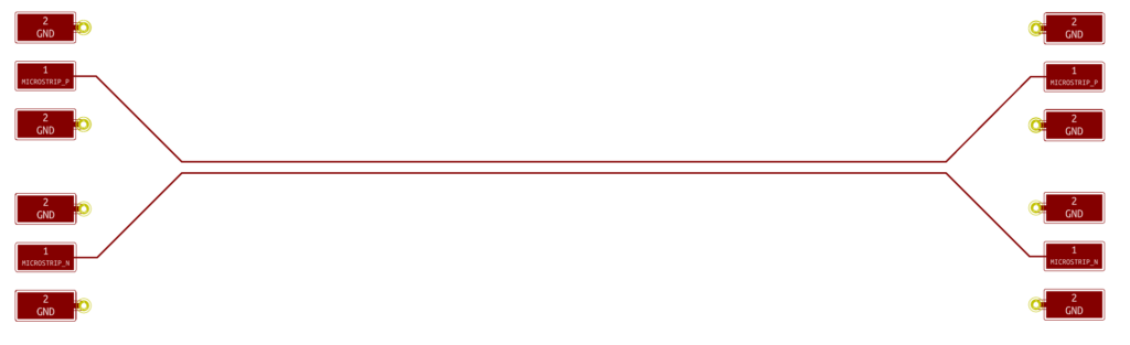
I’ve choosen multiple transmission line derivats:
- Coplanar (Single / Differential)
- Stripline (Single / Differential)
- Microstrip (Single / Differential)
- 90° corner with a coplanar waveguide
- Impedance controlled via
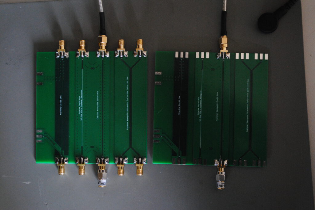
I designed a layout with simple sma edge connectors and the transmission lines according to the calculations.
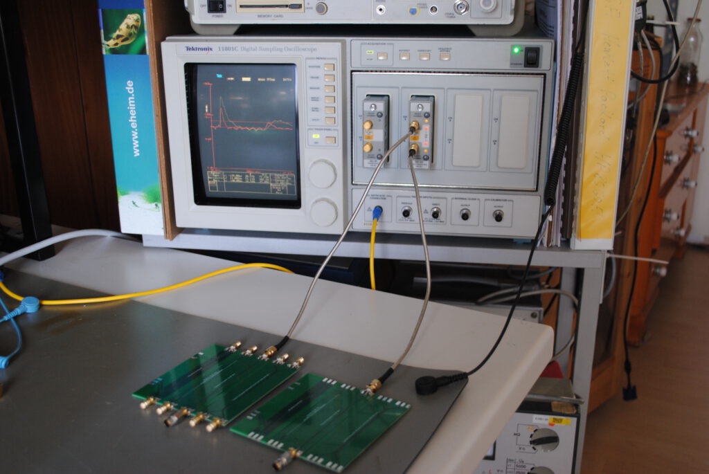
Measurements & Rework
And … the measurements showed ‚horrible‘ results. Let’s have a look at the coplanar waveguide:
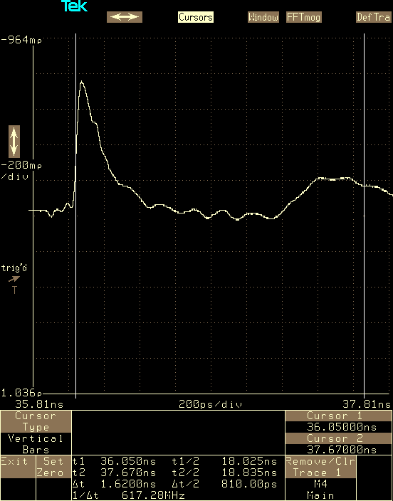
On the right hand side one can see that the impedance variation is for (calculated 50 Ohm) pretty okay +7/-3 Ohm, but at the start and the end there are huge impedance discontinuitys.
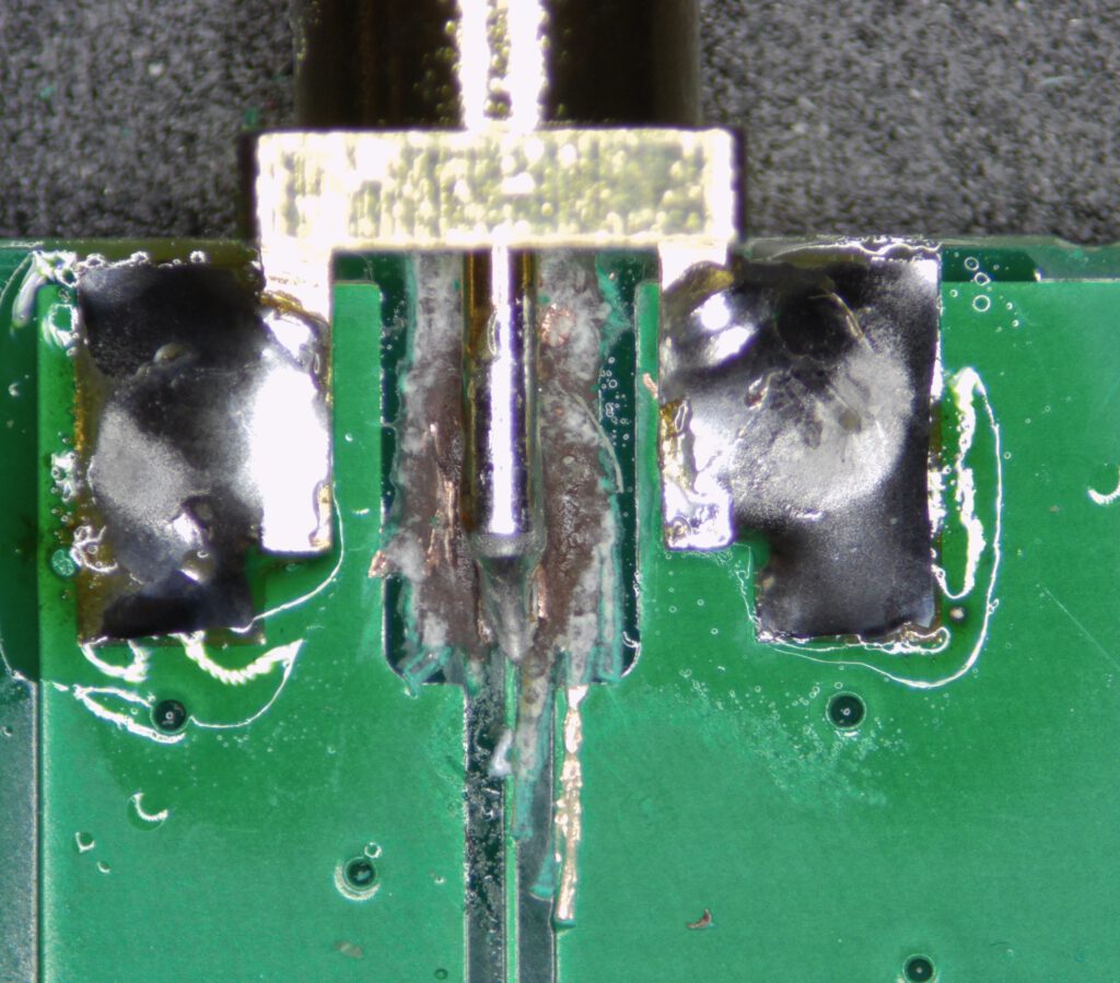
I thought so long about the transmission line itself, that I completely missed out on the connection.
As a no-brainer I slapped some SMA edge connectors on there and didn’t care further.
The main issue here is this region:
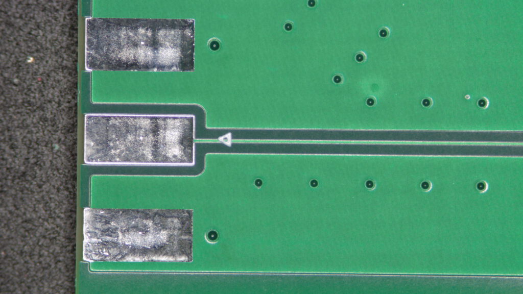
Those SMA edge connectors (or at least this footprint) are mainly designed for 2-layer PCB designs where the impedance for 50 Ohm is roughly this pad size
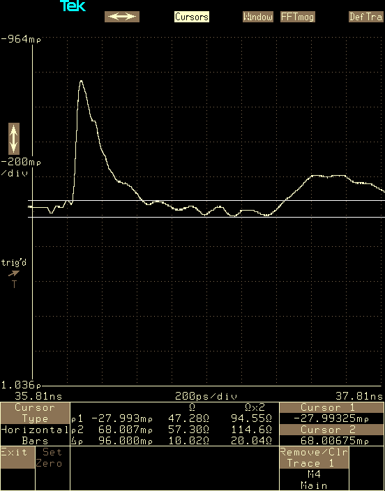
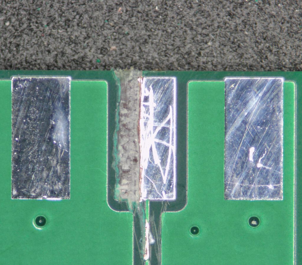
I evaluated my guess by cutting the pad size down to the width of the trace
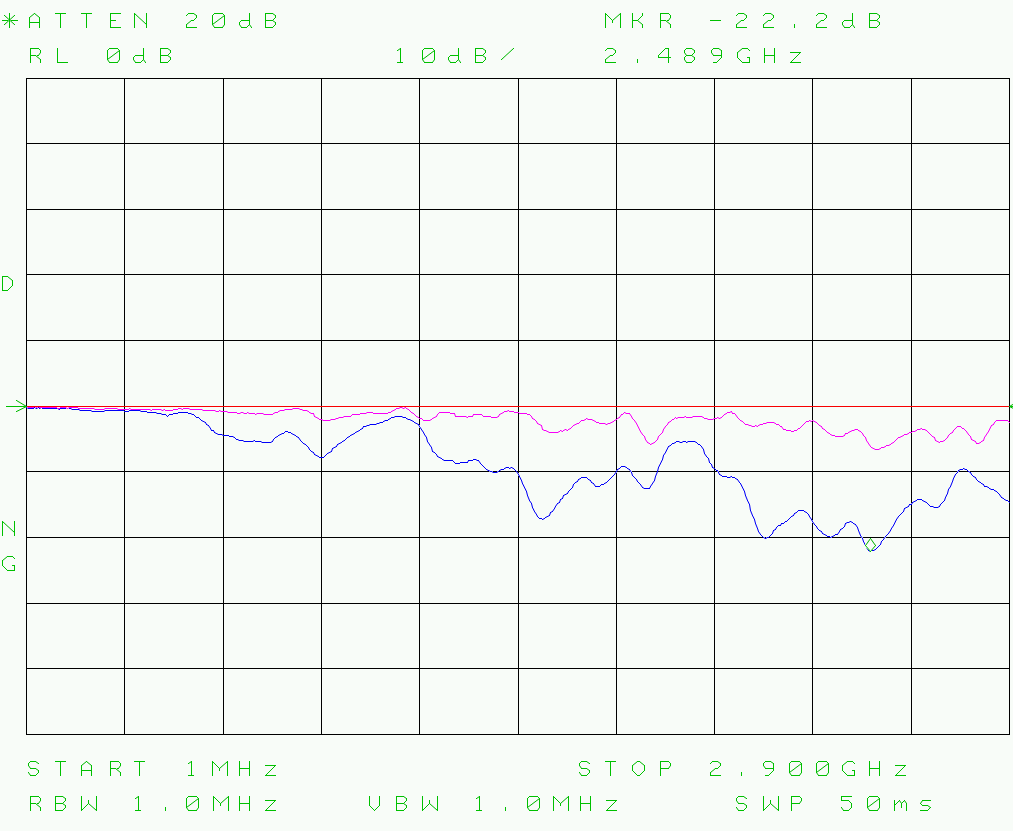
Here a before & after screenshot of a S21 measurement with the HP8560A up to 2.9GHz.
The blue trace is the PCB as designed; the pink trace the measurment with the rework.
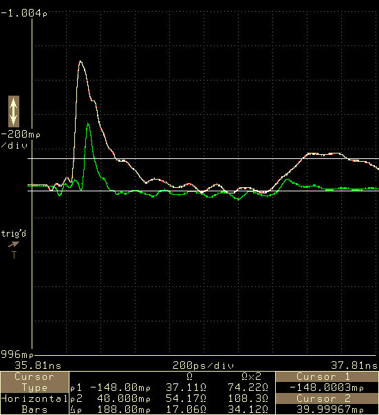
And here the TDR comparison of the 11801C:
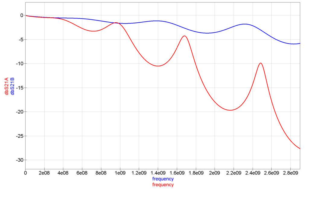
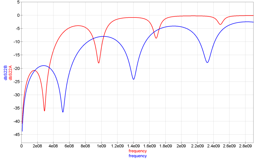
Simulation when it was too late
I tried to simulate the results with Qucs I’ve got the following results for the reworked and original
Super!
Ich staune über diese Arbeit.
Außerdem ist genügend Fachwissen vorhanden, komplexe Elektronik zu reparieren!
Respekt!
Viele Grüße
Michael