
Introduction
The fundamental idea behind this project is, to pimp up the design concept of my personal personal exam part one of my apprenticeship as an electrician.
Design of final exam
The final exam design’s purpose was to have a simple test device for measuring breakthrough voltages of different types of diodes.
It had the following features:
- Three different current settings (1mA, 5mA, 10mA) up to 10V
- Voltage reading with 8-bit resolution
- Two digit seven segment display
As I had the need for a current source for testing multiple high power leds, I thought about cranking the old design.
But in my opinion nearly all „features“ were insufficient.
Initial idea
I had the Texas Instruments XTR110AG lying around, and found the IC interesting enough to design a circuit around it.
Under normal circumstances this device is meant for adapting 0 – 5V or 0 – 10V analog sensor signals to 0 – 20mA or 4 – 20mA.
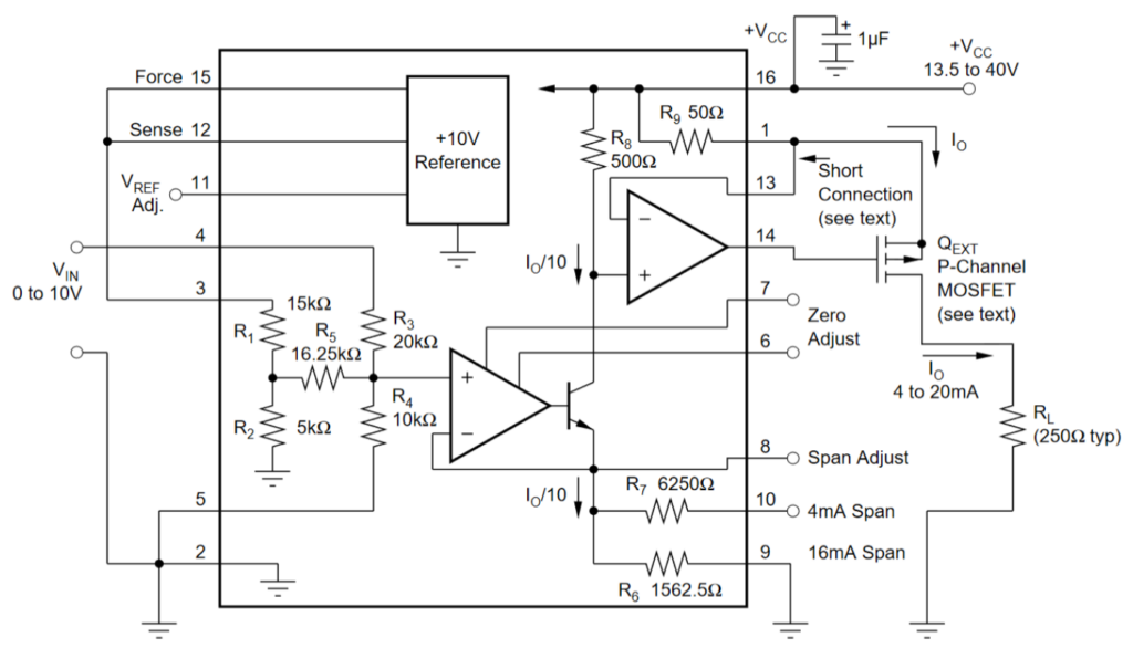
But by switching the current shunt resistor for a smaller value(R9 in schematic), the upper range limit can exceed 20mA.
Also the voltage input was perfect for interfacing with a MCU of any sort.
Revision 0.1
Desgin decisions
All resistors were designed to take coal film resistors (5% tolerance) out of my standard assortment.
Most parts, like the XTR110AG, were choosen because I had them on hand and not for their best fit into the curcuit design.
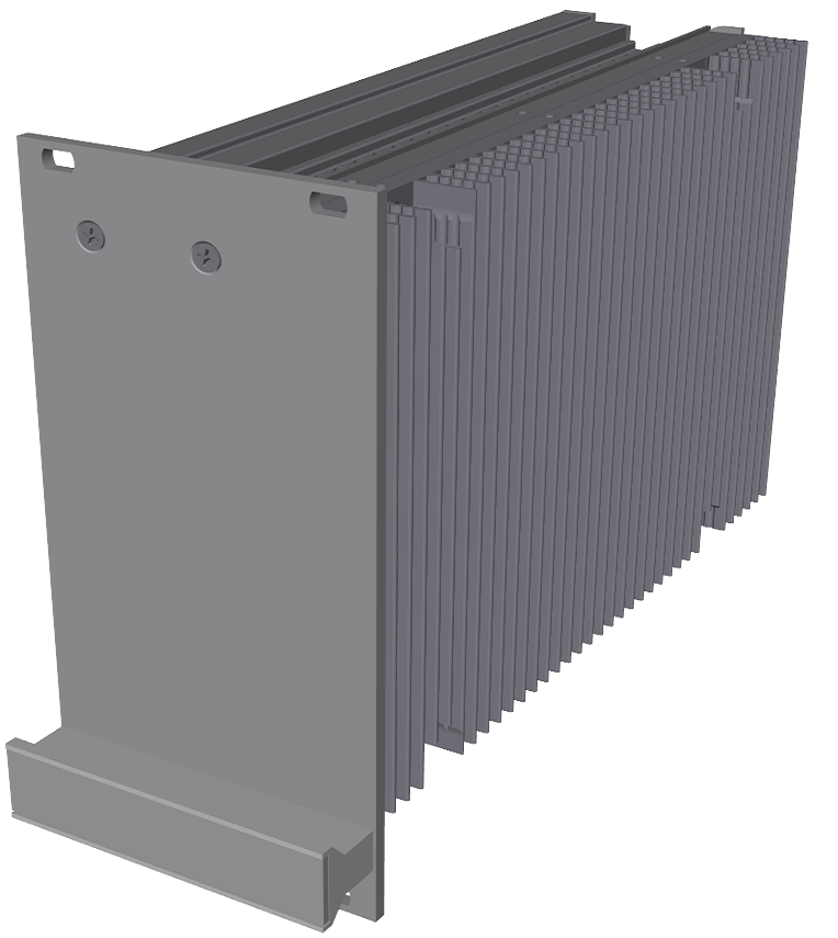
Mechanical
My wish was to let this PCB be in the dimensions of the widespread (in Germany) „Europa Karte“, specifically speakin 100mm x 200mm.
Connection wise I’ve choosen the DIN41612 (according to the „Europa Karte“) H15, 15 pins which allow a current up to 15A.
The form factor of the pcb will allow easy ordering of housing with a front panel and integrated cooling solution.
Analog part
The maximum input voltage was oriented to the maximum output voltage or supply voltage the XTR110AG can deal with, 40 Volts.
The input attentuation was designed to be adjusted to a damping factor of eight.
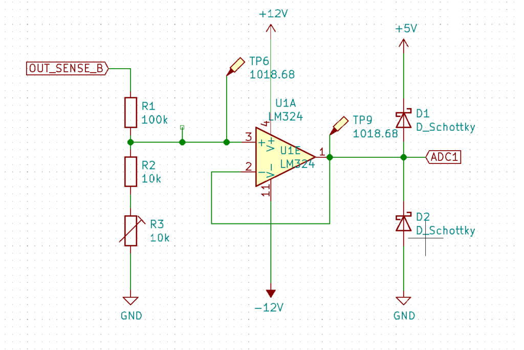
In my personal stupidity I precisely and fine selected the cheapest operational amplifier to find in my components assortment.
The mighty and lovely LM324 as the Germans tend to call „forest and meadows“ – op.
The OP was wired up as buffer.
Digital part
For control of the shunt switching, readout of the ADC, adjustment of DAC etc…, I’ve choosen an Arduino Nano.
Mainly for the simplicity and some sweet librarys like Vrekrer SCPI Parser.
The GPIOs of the Arduino were extended via a PCF8574.
Building
Build up of the PCB after arrival was seemlessly, except the one and only connection I’ve forgot to route at layouting.
It was the feedbackloop of the first lm324 buffer amplifier. So it was an easy fix with a big solder bridge betw:een pin 1 and 2 of U1A.
Firmware
Measurments
The data was captured with a little pyvisa supported python script, utilizing the SCPI (virtual serial port ~ USB) interface of the constant current source.
The sampling factor in the firmware was 10.
Stabilitiy of voltage measurment over 2 hours
The measurment was done by connecting the voltage inputs directly to the reference voltage source. Here we can see what is later further confirmed:
Measurment on channel A is much worse than channel B.
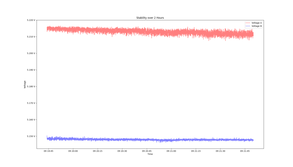
Channel A
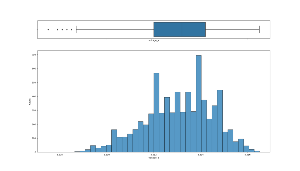
| Value | Measurment |
|---|---|
| Standard Deviation | 1.456 mV |
| Maximum Value | 5.216500 V |
| Minimum Value | 5.207500 V |
| Mean Value | 5.213059 V |
| 25% of Counts | 5.212000 V |
| 50% of Coutns | 5.213200 V |
| 75% of Counts | 5.214200 V |
Channel B
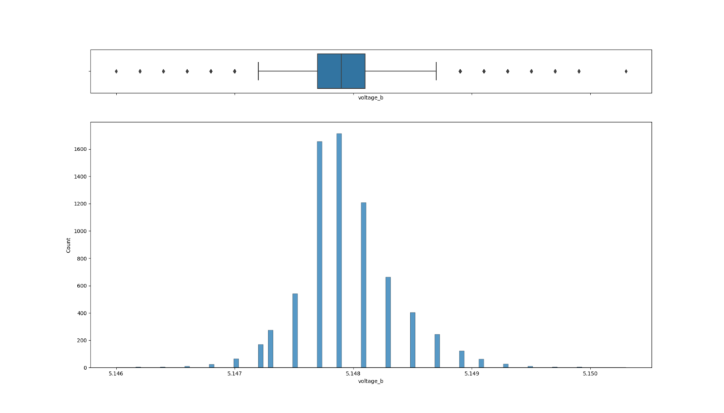
| Value | Measurment |
|---|---|
| Standard Deviation | 411 uV |
| Maximum Value: | 5.150300 V |
| Minimum Value: | 5.146000 V |
| Mean Value: | 5.147937 V |
| 25% of Counts: | 5.147700 V |
| 50% of Coutns: | 5.147900 V |
| 75% of Counts: | 5.148100 V |
Stabilitiy of voltage measurment over 24 hours
As an introduction to these pretty „special“ values:
- The PCB is black
- Biggest temperature rise at this day was between 10am and 1pm
- The sunlight hit the pcb directly
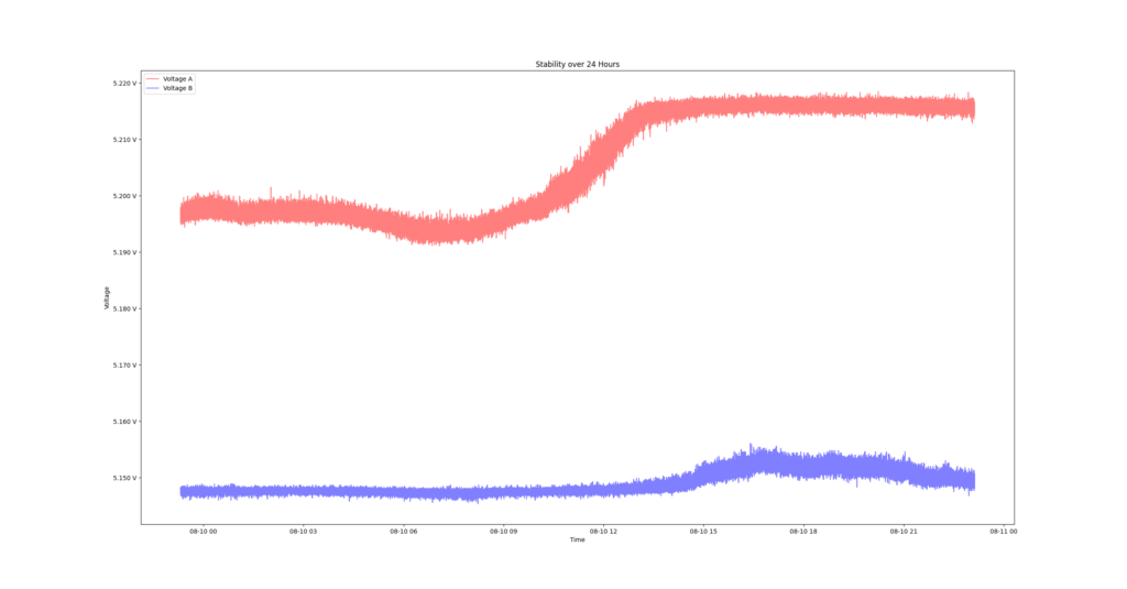
But also this measurment questions the inputamplifier at all with his voltage divider. So far I have no explanation for the non-drift of the channel B.
Also the stability ios better after the temperature drift.
Channel A is much more stable after the rise in temperature even the temeprature has fallen after 3pm.
But channel B gets more drifty in this szenario.
Result and outlook
In longtime tests the voltage divider at the input stage performed poorly:
- Bad resistors (coal film resistors)
- Bad design, the trimm potentiometer drifts enormous
- The attentuation of 8 got me in every voltage range just a resolution of 40V / 2^12 = 9.7mV best case. Which is not that grate deal, but with a simple range switching to damping 1, it can be greatly improved.
Also the zeroness of the operational amplifier with a base offset voltage of 1mV – 2mV meant, that without offset adjustment I’am loosing best case one ADC step.
At all I forgot totally the functionality to measure the real current.
If
I = U / R
I constant:
R -> ထ  ; V -> ထ
So if the maximum voltage of the power supply is 40V, at some point the constant current source can’t keep up with the load.
But it is necessary to monitor the real current flowing.
In the next design I’ll include a measurment over the shunt used by the XTR110AG.