Together with a signal generator (a Marconi 2032) I got my hands on an old (~2003) sattelite out door unit. These rugged units – the case itself probably weighs like 10 kg – are usually as the naming may imply mounted outdoor in close proximity of the parabol sattlite dish. The main reason is to keep the 29 GHz (KA-Band) signal lines as short as possible and do the actual data transmission at a much more reasonable intermediate frequency.
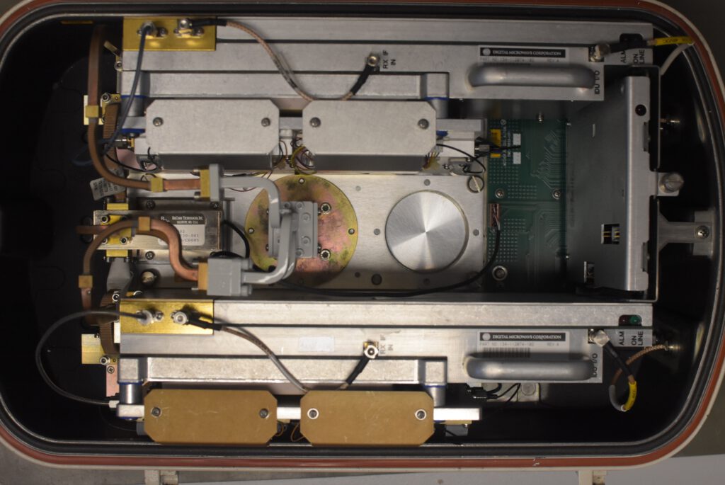
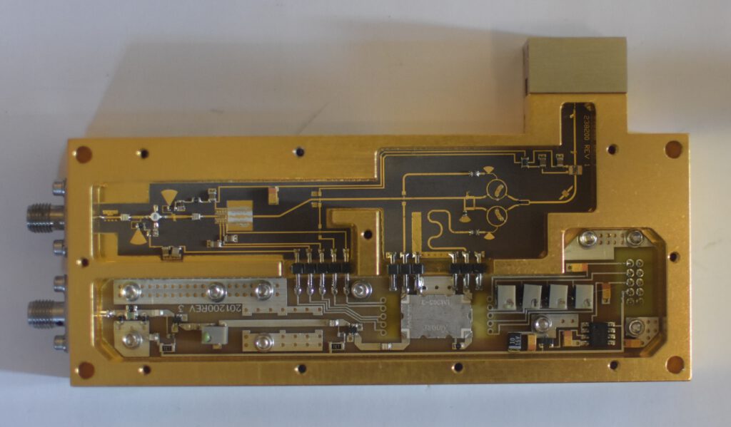
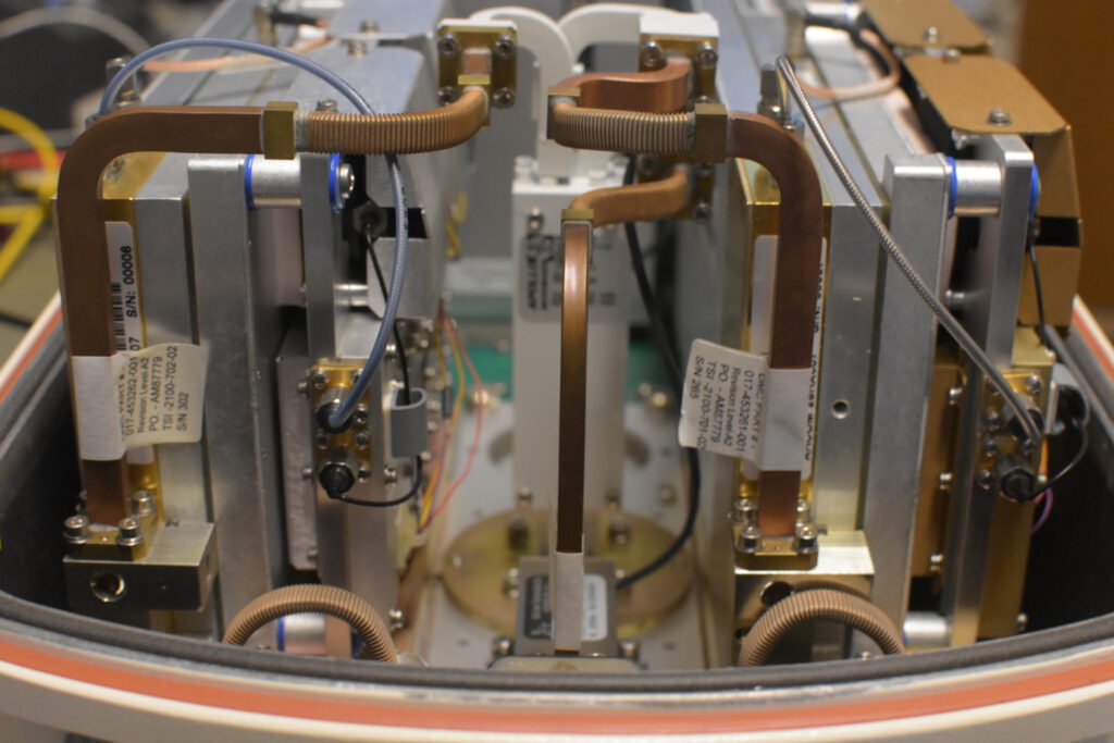
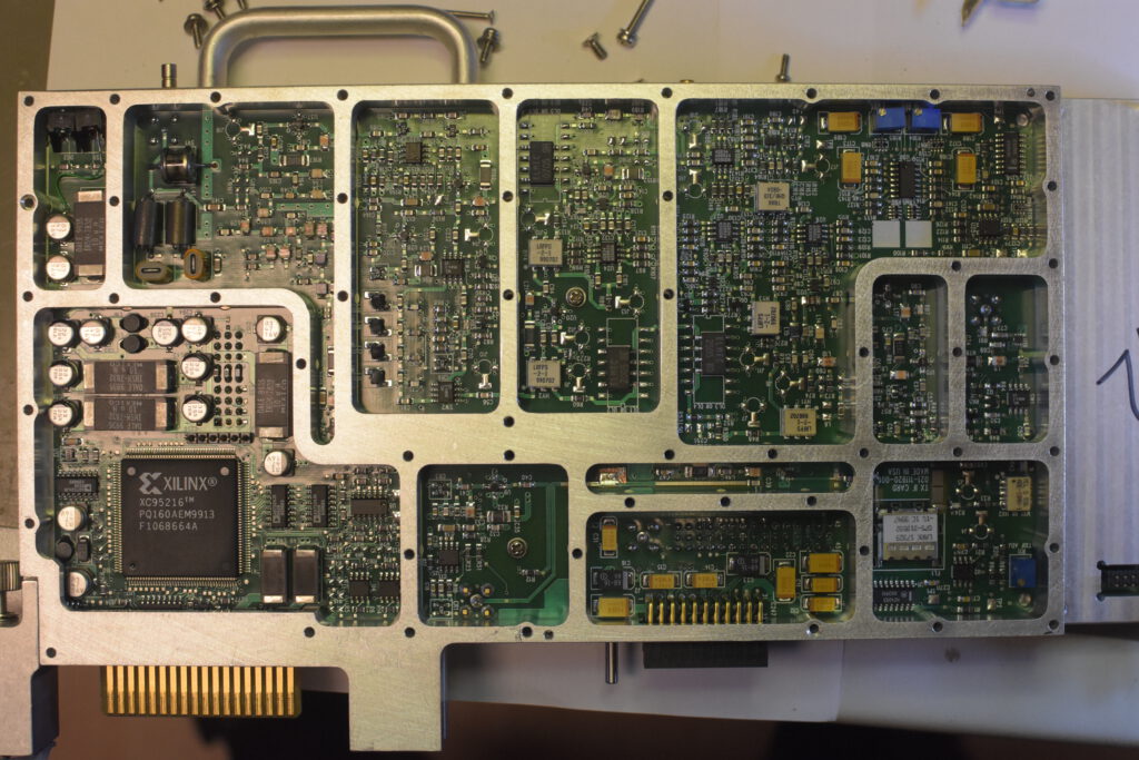
The unit consists of two independent transmit and receive units which can receive simultaneously but only one can transmit. Selected by the SPDT WR28 waveguide switch on the leftside on the upper image.
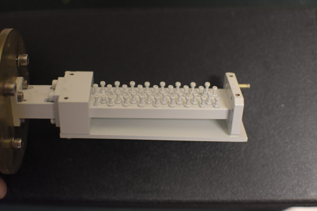
Prominnently placed in the middle is the diplexer preselecting the receive and transmit frequency ranges. The transmit frequency is at 29013 MHz and the receive band at 28005 MHz. The cconnection to the waveguide feed would be through the backside of the unit via a flush watertight waveguide interconnect.
Receive section
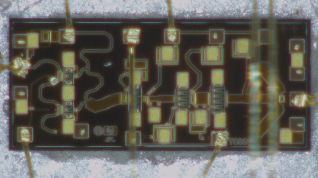
Closer inspection of the receive assembly reveals a rather simplistic 1st down conversion with the carrier and a single sideband (SSB) demodulator with two microstrip double balanced mixer with a microstrip 90° hybrid.
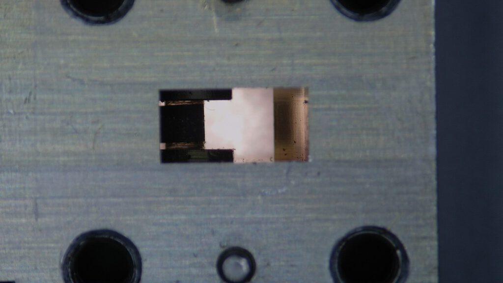
The waveguide incorporates an isolator (probably for reflection suppression). The input gets amplified by a HP (Keysight) TC906 MMIC amplifier.
The carrier signal chain undergoes a initial gain stage and gets than trippled by a TC906 in multiplier configuration (higher harmonic amplification) and then filtered to the receive carrier of 29 GHz.
The intermediate frequency gets ampliefied by two gain stages after the 90° hybrid.
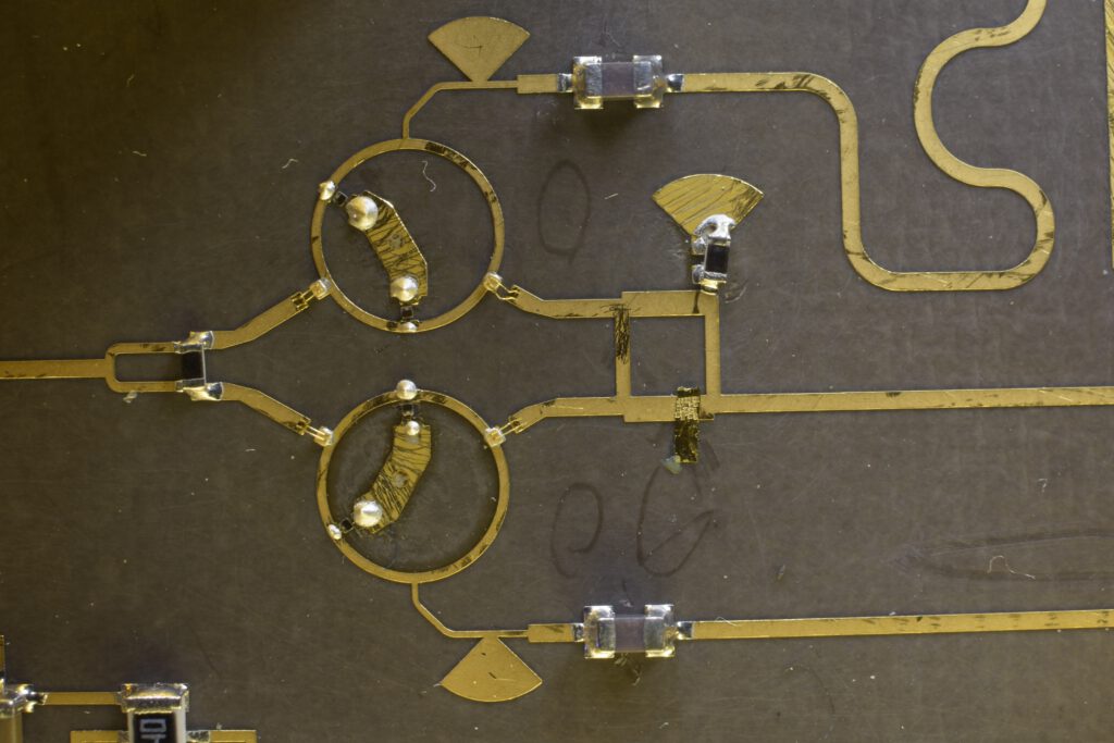
and Microstrip 90° Hybrid
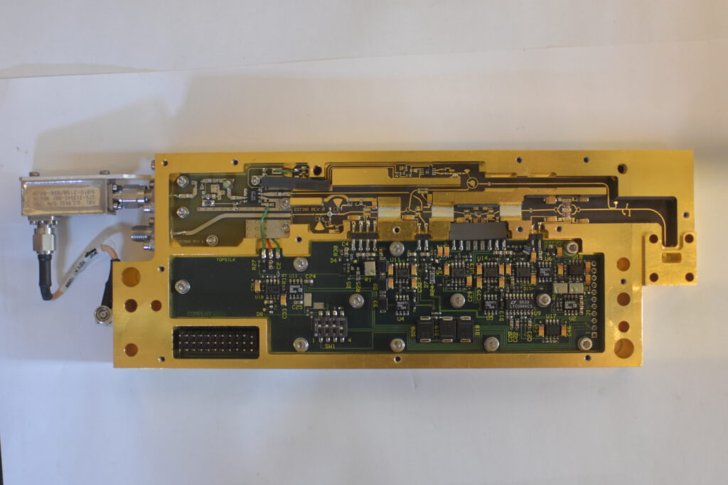
Transmit Section
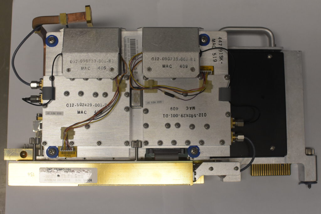
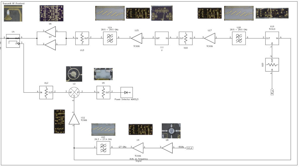
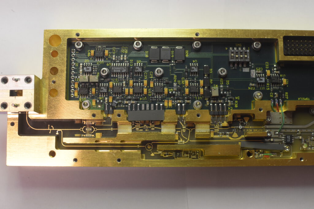
The RF frontend for the transmitter is slightly more complex. It composes a carrier cleanup and amplification, modulation with the IF signal and power detection feedback path for power adjustment.
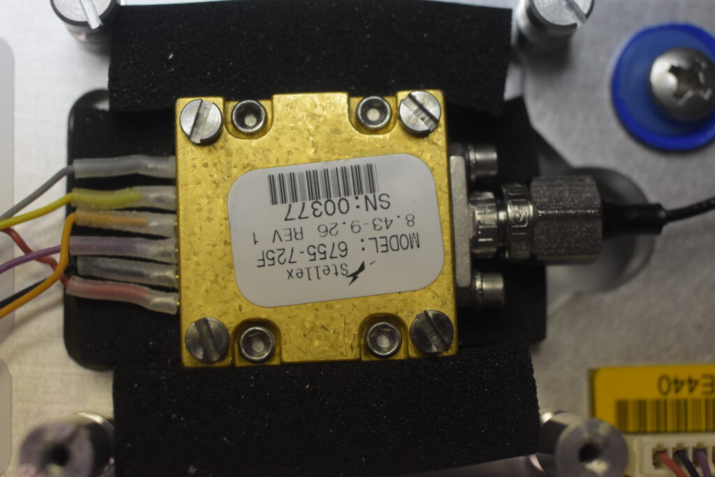
The carrier frequency section consists of a frequency trippler to get the around 9.3 GHz signal from the YIG tuned Stellex VCO to the 28 GHz and amplify it and filter it.
Further the carrier is used to down-convert the coupled signal of of the transmit ouput to bring the signal to frequency the AD8313 logarithmic detector is capable of.
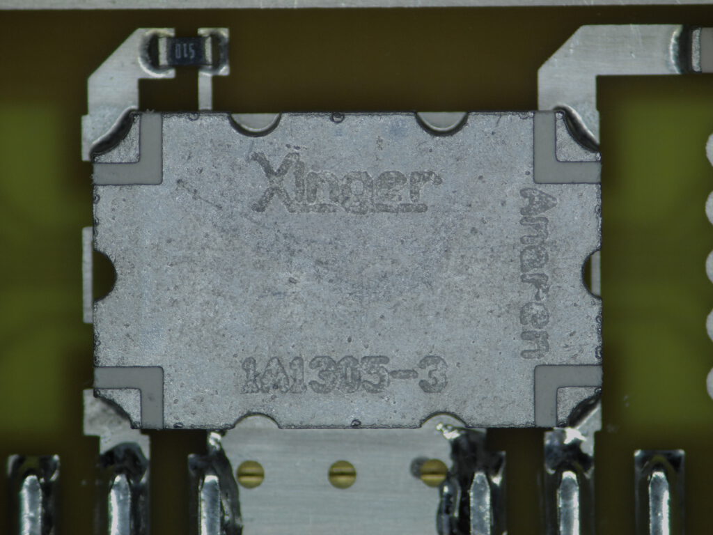
All mixers on these boards are built with microstrip balanced mixers with two diodes in a ring-structure.
The intermediate frequency from the IF assembly is cleaned up with an external K&L bandpass centered at 2.15 GHz with a span of 500 MHz. The further IF gets amplified and then modulated onto the carrier via the the HP TC913 MMIC. I haven’t found any datasheet on this chip, but would expect either a SSB modulator or just a plain mixer. Furthermore the signal chain sees amplifier-filter combination multiple times until it hits the power amplifier stage at the end with two parallel amplifiers fed by a power splitter and then again combined via a resistive power splitter.
The output is (not shown on the assembly photo down) fed into a waveguide ciruclator.
Probably to reduce reflections that would hit the power amplifier stage which shouldn’t be to resistant to reverse power.
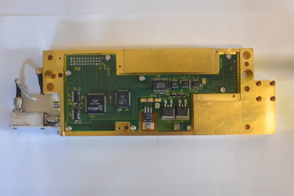
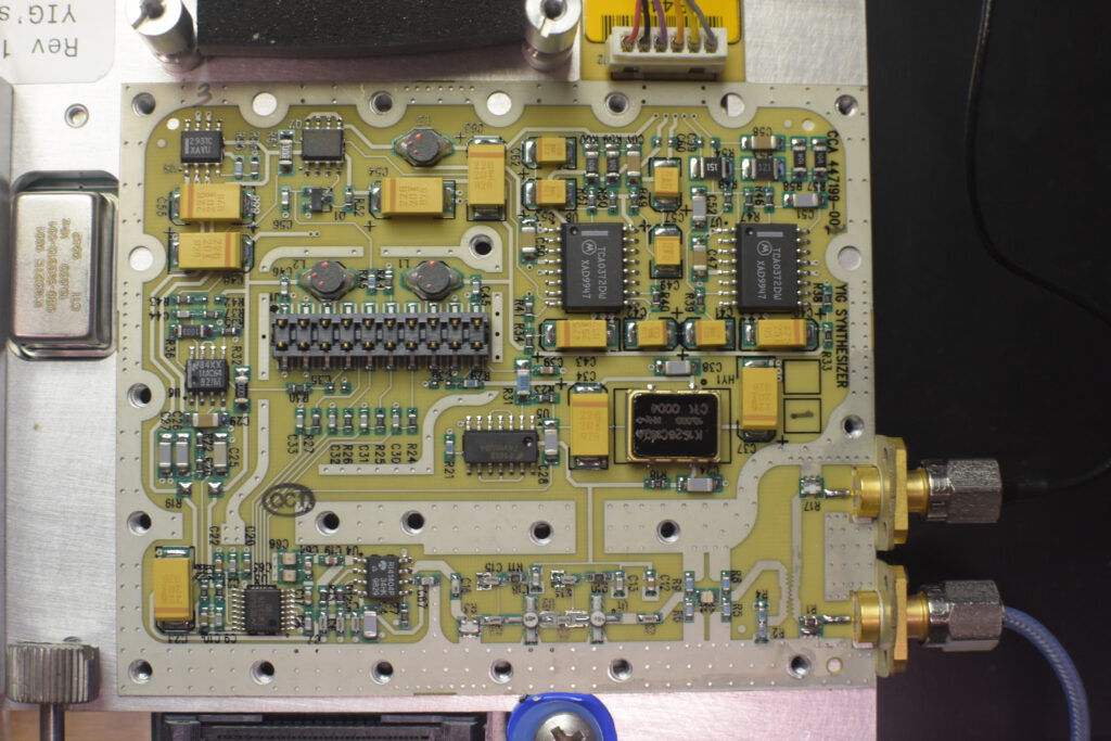
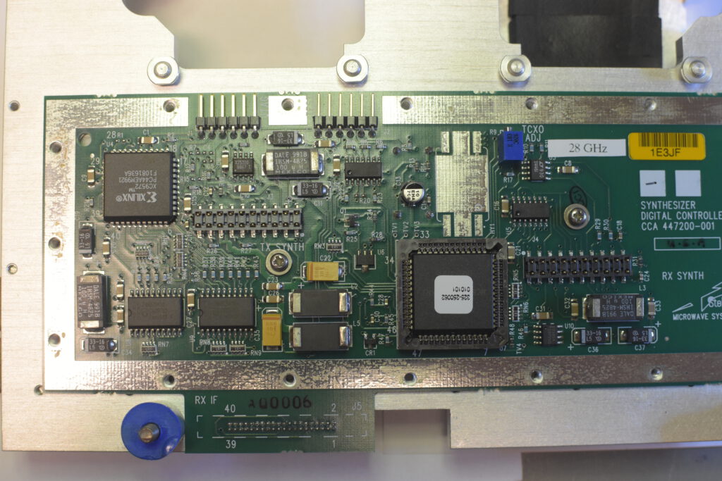
The control board on the back consists of a double multiplication DAC with a Lattice CPLD and some EEPROM.
I suspect due to the internal wiring between the OP amps and the DAC that these are used for envelope tracking. Enevelop tracking basically just drives the amplifiers with low supply voltage when no data is transmitted and high voltage when transmitting. This is done to save dissipated and used power by the transmitter. For example this transmit assembly is sticked to the complete hull of the ODU which incoporates a 50 by 20 cm passive coolter. These KA-Band transmitters are even with envelope-tracking not too power efficient.
Teardown Pictures

Stellex YIG Tuned Oscillator Teardown